Raman spectroscopy is highly sensitive to subtle changes in the crystal lattice structure of semiconductor materials. When a semiconductor is subjected to stress (by pressure, tension, or some other sophisticated method) during manufacturing, its molecular bonds shift slightly, changing the lattice vibration frequency. By measuring these subtle shifts in the Raman spectra, the intensity and type of strain present in the semiconductor material can be inferred. Such information is essential in semiconductor manufacturing technology, as even small amounts of strain can significantly affect (positively or negatively) the properties of the material and consequently the quality of the manufactured device.
The production of integrated circuits involves many steps, including various types of treatments and the formation of nested microstructures, which also involves the deposition of materials with different crystal lattices and thermal expansions. These steps in the production process can lead to the development of stresses leading to deformation of the materials. Stress in semiconductors leads to changes in optical and electronic properties, such as changes in nonlinear optical phenomena, band-gap and electron carrier mobility. It also affects the propagation of dislocations, the formation of cracks and cavities. In some cases, however, stresses are intentionally built into semiconductor materials to improve some specific properties. In both cases, it is necessary to have measurement technology available to monitor and optimize these phenomena during semiconductor production.

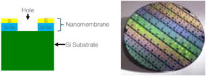
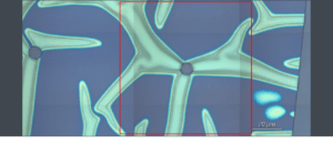
The sample in the picture is a heteroepitaxial layered semiconductor. A nanomembrane of 41 nm thick Si-Ge layer is deposited on a silicon substrate and then covered with another 23 nm thick layer (Epi layer) of silicon. The mismatch between the crystal lattice of the Si-Ge and silicon (Si) layers results in strain. As part of the finalization of the production, the lower silicon substrate (Si Substrate) is finally removed, but in this example, the resulting nanomembrane has not yet been released from the substrate for Raman imaging. This causes the “wrinkles” observed on the sample. The dark circle in the middle of the “wrinkle” is a hole in the semiconductor nanomembrane, which allows access to the silicon substrate and is part of the process to finally release the nanomembrane from the Si substrate.
The measured area of the layered semiconductor is 62.5 μm x 67.9 μm, mapped using a DXR3xi Raman imaging microscope with a 455 nm excitation laser (pixel size for imaging was 0.1 micrometer, 100x magnification objective used).


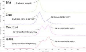
The colors of the resulting imaging visually represent the shift in the location of the silicon peak. The white color corresponds to the standard location of the 520.7 cm-1 band of the silicon substrate (the hole in the middle of the wrinkle), the darker the colors, the more the 520.7 cm-1 band of silicon is shifted to lower wavenumbers (yellow 518.8 cm-1 to black 512.4 cm-1). The greater the shift of this silicon vibration, the greater the strain.

Further reading:
Maximilian Ries, Fabian Heisinger: Using Raman spectroscopy to determine the strain in semiconductor samples, Thermo Fisher Scientific Application note
Robert Heintz, Alexander Rzhevskii: Evaluating Silicon using Raman Microscopy,
Thermo Fisher Scientific Application note
