Modern nanotechnology does what nature has always been able to do: using sophisticated techniques, it creates new materials with new properties. One of them is semiconductor building blocks for high-speed electronics. To understand the behavior of these structures and to make them even faster, smaller, and more efficient, we need to know how electrons move on the length scales of only a few atoms. These processes are often extremely fast, prompting efforts to develop a microscope that combines excellent spatial resolution with the highest possible temporal resolution: the neaSCOPE THz microscope with femtosecond time resolution.
The neaSNOM microscope achieves excellent spatial resolution by focusing light on a small metal tip. As a result, the radiation is amplified only in a small volume, in an area only 10 nanometers wide in all three directions.
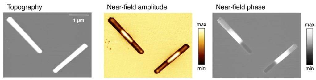
The tip collects and restricts light to a volume that is billions of times smaller than in conventional optical microscopy. The tip is then rasterized across the sample surface and the incident light that is scattered depends on the local properties of the sample directly below the tip. In this study, the tip is illuminated by infrared flashes of light lasting only a few femtoseconds. Femtosecond is an incredibly short fraction of a second. To detect the scattered light with the highest possible time resolution, the neaSNOM microscope uses incredibly fast sensors that can also observe infrared light oscillations.
As in slow motion movies, these flashes of light allow you to take pictures of super-fast electronic nano-motion. In a spectacular demonstration experiment, scientists were able to record a 3D film of moving electrons on the surface of a semiconductor nanowire, which was previously only available indirectly.
Such nanostructures, which were manufactured at CNR – Istituto Nanoscienze in Pisa, are very interesting for future high-speed electronics. In addition to answering technological questions in electronics and photovoltaics, neaSCOPE microscopes are also valuable for a wide range of interdisciplinary applications, ranging from providing new physical perspectives on exotic materials to understanding biological processes at the molecular scale.
You can learn more about this and other applications here.


