- Application description
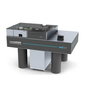
- neaSCOPE product line
With IR nano-imaging, you can directly map the concentration of free carriers at the nanoscale, giving you a strong contrast between the conductive and isolation phases. The method is completely non-invasive and without any artifacts caused by the so-called mechanical or thermal crosstalk.

IR nanoscopic data measured at given sample temperatures during the phase transition of the insulator to metal (VO2). After heating, the nanoparticles of metal regions nucleate (green), then grow with increasing temperature and finally merge together. Such measurements provide a new perspective on VO2 by analyzing separately the structural and electronic properties and with them it is possible to monitor the effect of local voltage or defects on the localization of electrons.


