Laser THz emission microscopy LTEM (Laser THz emission microscopy) in the near field (SNOM)
Terahertz radiation is an electromagnetic wave that lies between microwave and infrared radiation, with frequencies of the order of tenths of a Terahertz (0.1 THz corresponds to a wavelength of 3 mm) to tens of THz (10 THz corresponds to a wavelength of 30 µm); Figure 1. This radiation at the border of optics/photonics and electronics has found its place in many scientific fields and practical applications. We can mention, for example, medicine (from cancer research to DNA analysis), natural sciences (research into the properties of solid substances such as superconductivity, magnetoresistance or transport phenomena; in the case of time-resolved THz spectroscopy, the physical essence of the mentioned phenomena can even be investigated), forensic analysis or product quality verification, as well as researching the phenomena with which he works, e.g. spintronics, investigating the possibilities of storing and transmitting information through the spin of electrons.
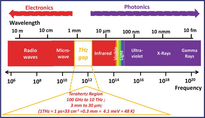
Figure 1: The electromagnetic spectrum
(William Ghann and Jamal Uddin: Terahertz (THz) Spectroscopy: A Cutting‐Edge Technology)
THz emission spectroscopy (TES) is a relatively new method of modern spectroscopy that uses THz waves to probe materials. In most cases, the source of THz radiation is the measured sample itself; thanks to the so-called excitation radiation. With the emitted THz waves, information can be obtained not only about the process responsible for this emission (optical rectification, shift currents, charge transfer, etc.), but also about other processes that can, on the contrary, “compete” with the generation of THz waves, and thus prevent the emission of THz radiation sample.
Laser THz (terahertz) emission microscopy (LTEM), a modern variant of this technology, is a method of so-called imaging, which in the last few years has become a powerful tool for the study and localization of electrical faults in integrated circuits, research and quality control of photoconductors, nonlinear optical crystals (ZnTe, GaP, etc.), evaluation of surface and interface properties in silicon-based systems such as Si-MOS, perovskite semiconductor research, etc.
Excitation of THz radiation in the sample is usually done by photoexcitation with an ultra-fast pulsed laser; the measuring system subsequently detects local variations of the emitted THz radiation with a very high spatial resolution. This resolution is usually less than 1 micron and is mainly dependent on the focusing of the excitation laser beam, e.g. with the lens used. Another revolutionary step to radically increase the spatial resolution of LTEM imaging is the combination of this measurement technique with s-SNOM technology. This measurement technique combines classic AFM (atomic force microscopy) with spectroscopy. Electromagnetic radiation (excitation) is focused on a sharp metal AFM tip located at a nano-distance from the sample surface, and during automatic mapping, scattered radiation is detected among other things. The used AFM tip thus functions as a nano-probe and the spatial resolution is then directly dependent on its size. s-SNOM has a very significant impact especially in analyzes that use the infrared region of the spectrum, where it can be considered as classical infrared (IR, FT-IR) microscopy, but with an exceptional spatial resolution below 10 nanometers.
However, the connection of short-wavelength THz radiation with an AFM tip at the nanoscale is very challenging, which usually prevents the study of new semiconductor materials with a large width of the so-called band gap – especially structures such as GaN/AlGaN/AlN/Si etc. In this study, the first successful measurement was achieved using a combination of LTEM and THz s-SNOM imaging techniques using energy higher than 3 eV, which here allows the use of a highly precisely focused blue laser (410 nm femtosecond pulsed laser) to obtain a spatial resolution in the order of nanometers (Figure 2).
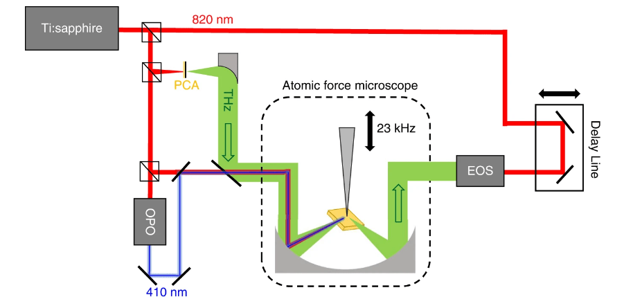
Figure 2: NIR radiation (820 nm), blue radiation (410 nm) and THz radiation are generated separately, THz pulses using a conventional photoconductive antenna (PCA). All three beams then converge at one point and focus on the AFM tip. Scattered and sample-emitted THz pulses are coherently detected by electro-optical sampling (EOS)
The result of this combined technique is the imaging of the samples (and the corresponding spectra) as well as the simultaneous LTEM image of the THz waves generated by the sample. When using 410 nm excitation, we generate terahertz pulses directly from the used silicon sample (bulk single-crystal), while this type of sample usually does not have an interesting emission of THz radiation when excited in the NIR region (near infrared region). Before the measurement, the silicon sample used was subjected to boron ion implantation with subsequent heat treatment (annealing) of the impurity in the implantation area, so the sample after treatment contains two areas of very different doping densities, with a relatively sharp boundary between them. The unimplanted region is simply an unmodified Si substrate that is only lightly n-doped (concentration ca. 1016 cm-3), while the boron-implanted region is p-doped, with a higher nominal doping density (ca. 1018 cm-3). The following Figure 3 describes one of the many outputs from this experiment.
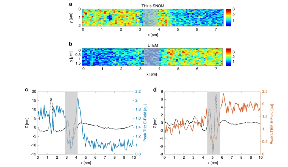
Figure 3:
- a) 2D THz s-SNOM image around the substrate/implant border
b) LTEM image around the substrate/implant border
c) Average line profile of THz s-SNOM (a).
d) Average LTEM line profile (b)
Note: Gray shaded areas indicate the border area where there is significant topography